PTA facilities for Metrology
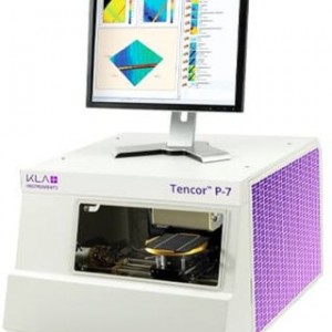
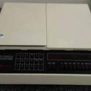
Metrology – Profilometre : KLA P7
Profilometre : P7
Metrology - Tools at a glance
Metrology field
2 Scanning electron microscope (2 Zeiss Ultra+ )
1 EDX (XFlash® detector 5030)
3 Optical microscopes (LEICA with digital camera)
2 Spectroscopic ellipsometer
1 Mechanical profilometer
2 reflectometres
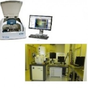
1 FPP-5000 4 POINT PROBE
1 AFM Icon Bruker
2 Scanning electron microscope (2 Zeiss Ultra+ )
1 EDX (XFlash® detector 5030)
3 Optical microscopes (LEICA with digital camera)
2 Spectroscopic ellipsometer
1 Mechanical profilometer
2 reflectometres
1 FPP-5000 4 POINT PROBE
1 AFM Icon Bruker
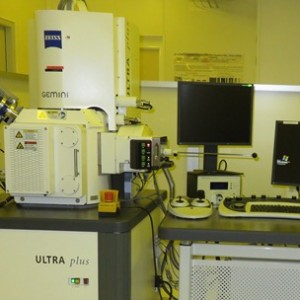
Metrology - MEB ZEISS ULTRA +
2 Scanning electron microscope : observation tools enabling enlargements up to x500,000 with a very great resolution.
MEB ZEISS ULTRA +
EDX (XFlash® detector 5030)
MEB ZEISS ULTRA +
EDX (XFlash® detector 5030)
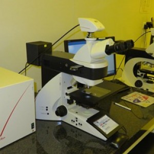
Metrology - Microscopes optical
Optical microscopes (LEICA with digital camera)
We have 3 optical microscopes LEICA (DM6000 and DM2500 at 1005 in CEA site and one DM2500 in the BCAi site) with Leica camera DFC 425 so, with a special solf, we can save samples images in tiff, jpg or bmp format.
We have 3 optical microscopes LEICA (DM6000 and DM2500 at 1005 in CEA site and one DM2500 in the BCAi site) with Leica camera DFC 425 so, with a special solf, we can save samples images in tiff, jpg or bmp format.
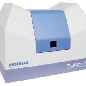
Metrology - Ellipsometre Auto SE + SpecEl
Auto SE
450nm to 1000nm : 450nm to 1000nm
Spectra resolution : Better than 3nm
SpecEI
Film Thickness Range: 1nm – 8μm
Thickness Resolution: 0,1nm
n & k Analyzer: Table 450 – 900 nm in 1nm steps
450nm to 1000nm : 450nm to 1000nm
Spectra resolution : Better than 3nm
SpecEI
Film Thickness Range: 1nm – 8μm
Thickness Resolution: 0,1nm
n & k Analyzer: Table 450 – 900 nm in 1nm steps
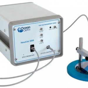
Metrology – Nanocalc-vis
Nanocalc-VIS Wavelength 400-850 nm
Nanocalc XR Wavelength 250-1050 nm
Nanocalc XR Wavelength 250-1050 nm
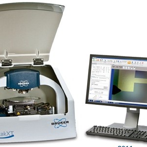
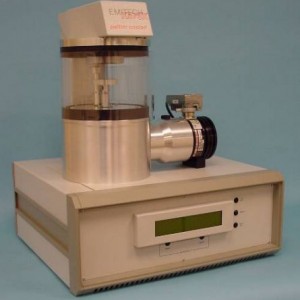
Metrology - DEKTAK DXT "E"
Mechanical profilometer: for measuring steps, the vertical resolution is 1Å
DEKTAK XT "E"
DEKTAK XT "E"
Metrology - 4 point probe FPP-5000
Metrology - 4 point probe FPP-5000
Metrology - K575X Sputter Coater
Métalliseur MEB
Metrology – AFM Icon Bruker
AFM