
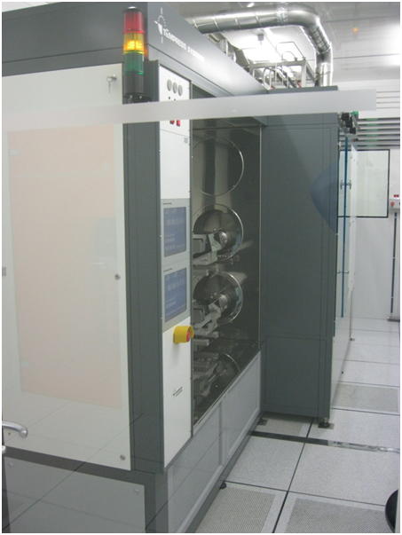
LPCVD Tempress
TECHNICAL DESCRIPTION:
Nitride silicon and polysilicon depositions
Temperature deposition : 600°C – 850°C
Pressure range : 150 mTorr
Gaz used : siliane, dichlorosilane, phosphine-silane mix, ammoniac.
Size and type of samples : 2inches and 4 inches bare silicon wafers only
Batch of 20 wafers can be processed in one run
PROCESS CAPABILITIES:
Gaz used :
- SiN : NH3 (amoniac), DCS (dichlorosilane)
- polysilicon : doped or non doped : SiH4/PH3 1% (silane/phosphine) or SiH4 (silane)
Thickness range : from 50 nm to 100 nm
Deposition rate range : ~5nm/min, regarding temperature and gaz flow
Process capabilities
One of this stack is dedicated to silicon polycristallin deposition, undoped or phosphorus doped.
The other stack is made for nitride silicon, low stress or stoechimetric.
 Polysilicon process
Contact: delphine.constantin@grenoble-inp.fr