
Lithography – Electronic beam lithography : JEOL6300FS
TECHNICAL DESCRIPTION
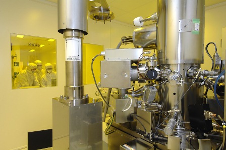
. Gun TFE electron beam source 100kV with 2 modes (High speed or High resolution)
. Laser control for the stage λ/1024 =0.62nm.
. Maximum frequency : 12MHz
. Field Stitching <20nm
. Alignment if using full correction <15nm
. Height measurement on the sample
. Sample 5x5mm to 8’’ wafers (maximum writing area on 6’’)
. Autoloader with 10 cassettes
Ré-alignment
PROCESS CAPABILITIES
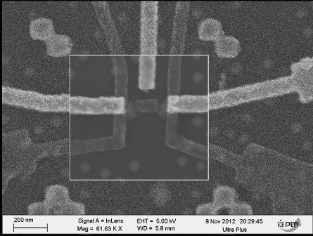
Positive resist
PMMA4% 950K, PMMA2% 950K, PMMA4% 200K
PMMA/MMA (for bilayer),ZEP520A or UV5-0.6)
Negative resist
XR-1541-004, Man2410 or NEB22A2
with a resolution in the resist less of 10nm.
The best resolution after a lift-off of Ni is around of 13nm.
Contact : jean-luc.thomassin@cea.fr