
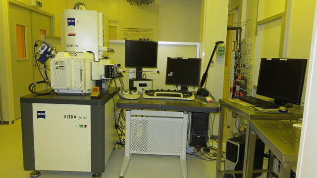
Metrology – MEB ZEISS ULTRA +
Technical description
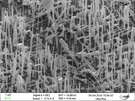
Resolution : 1.0 nm @ 15 kV, 1.7 nm @ 1 kV, 4.0 nm @ 0.1 kV
Magnification 12 - 1,000 kx in SE mode, 100 - 1,000 kx with EsB detector
Acceleration Voltage 2 kV - 30 kV
Standard Detectors
EsB detector with filtering grid , (0 – 1500 V) IntegratedAsB detector , High efficiency In-lens SE2 detector
Specimen Stage
5-Axes Motorised Eucentric Stage
X = 130 mm
Y = 130 mm
Z = 50 mm
T = -3 to 70°
R = 360° (continuous)
Echantillon : Wafer jusqu'à 4 ”
Image Processing
Resolution: Up to 3072 x2304 pixel , Noise reduction: Seven integration and averaging modes
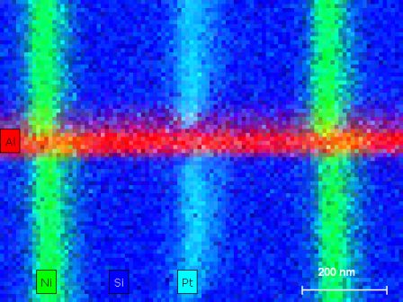
EDX (XFlash® detector 5030)
Technical description
Energy resolution : 127 eV at Mn Kα (54 eV C Kα, 64 eV F Kα), guaranteed up to 50,000 cps
Detection range : from boron (5) to americium (95)
Maximum input : count rate 750,000 cps
30 mm2 : active detector area
Peltier cooling : (neither liquid nitrogen nor water required for cooling)
Document :